1. 서론
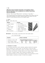
나노복합소재(Nano-composite)란 두 가지 이상의 나노입자들을 조합하여 각 재료들의 물리적, 화학적 성질을 합쳐 놓은 재료로서, 구성재료의 장점을 최대한 이용하여 성능을 개선시키고 특성을 서로 조합하여 원하는 특성을 얻을 수 있게 설계한 소재이다. 나노는 10-9m를 나타내는 수치로 머리카
Keff, Km, Kp : the effective thermal conductivities of the composite,
Metal matrix, Particles
φp : the volume fraction of reinforcements
a : the diameter of the reinforcement
- hc : the boundary conductivity.
Advantage
The air travels across the short
length of the fins laterally, rather than longitudinally down
the long length.
Focused on placing
resulting nanocomposites. However, the effective thermal conductivity of carbon-based nanocomposites is strongly influenced by the Kapitza interfacial resistance.
In this study, a comparison between carbon nanotubes and graphene sheet nanocomposites that takes into account dispersion patterns of the nanoinclusions and the Kapitza resistance is performed by means of a Monte Carlo simulation.
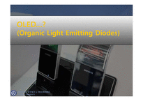
First, Substrate is consists of a plastic or glass, a portion of the OLED is supportive.Anode is a role that make electron holes when current flows by removing electron. And the upper Conducting Layer is the place that Electron Holes is being created.Emissive Layer is the place accepting an electron from Cathode and produce light.
Emissive layer and conducting layer are called organic layer beca
4. Condition
If reflow, IMC layer occurs between the solder ball and substrate. IMC layer's composition changes depending on reflow time.
Temperatuer
255℃
Reflow time
1s, 1min, 5min, 10min, 20min
Experimental conditions
5. Analysis
IMC layer change was observed according to the reflow time.(Reflow time : 1s, 1min, 5min, 10min, 20min). Do refer to